In the previous post we described a method of outputting a fixed bit pattern to a port pin. The method we used will work on all ARM chips - ARM7, ARM9 and Cortex-M3. The result was a single write instruction for each output bit.
In this post we will use the bit-banding of the Cortex-M3 core to achieve a fast output of a variable bit stream.
The Cortex-M3 core has two bit-banded regions:
1. on-chip SRAM space starting at address 0X20000000 and
2. on-chip peripheral space starting at address 0X40000000.
To read or write a single bit in the on-chip SRAM space we write into the bit-banded region starting at 0X22000000.
To read or write a single bit in the on-chip peripheral space we write into the bit-banded region starting at 0X42000000.
The ARM documentation give the algorithm to calculate a bit address. Using this information, we have defined four macros to simplify our coding:
#define byte_base_difference 0X20000000
#define byte_offset(a) (((unsigned long)&(a)) - byte_base_difference)
#define bit_word_offset(a, bit_number) ((byte_offset(a) * 32) + (bit_number * 4))
#define bit_word_addr(a, bit_number, bit_band_base) (bit_band_base + bit_word_offset(a, bit_number))
Now if we define a variable such as:
unsigned long nDWord;
the address of the first bit of this variable will be:
#define addrbit0 (unsigned long*)bit_word_addr(nDWord, 0, 0X22000000)
We can write a 32-bit value into nDWord using a normal assignment, and we can read it one bit at a time using the appropriate bit-band address. Using this method we avoid the need to do any shifting. (By the way, this method of avoiding shifts has been possible on the 8051 microcontroller for the last 30 years!)
Similarly we can use the same macros to define the address of a bit in an on-chip peripheral register. For instance the address of bit 12 of the EFM32 port A data out register is:
#define addrDoutPA12 (unsigned long*)bit_word_addr(g_pGPIO->PA_DOUT, 12, 0X42000000)
We can use this address to write to this bit and set or clear pin PA12. (Not forgetting to enable the GPIO clock and configure PA12 as an output using the GPIO graphical wizard.)
We can assign these addresses to locally defined pointers to ensure that the addresses are kept in registers:
unsigned long* pBit = addrbit0;
unsigned long* pPin = addrDoutPA12;
Then for instance to output bit 2 of nDWord to PA12, we can use a simple assignment:
*pPin = *(pBit + 2);
Here is a function that will write all 32 bits of nDWord to PA12:
void output_pattern(unsigned long nPattern)
{
nDWord = nPattern; // get the bit-stream bits into bit-banded SRAM
// local variables so that the reside in registers:
unsigned long* pBit = addrbit0;
unsigned long* pPin = addrDoutPA12;
*pPin = *(pBit + 0);
*pPin = *(pBit + 1);
*pPin = *(pBit + 2);
*pPin = *(pBit + 3);
*pPin = *(pBit + 4);
*pPin = *(pBit + 5);
*pPin = *(pBit + 6);
*pPin = *(pBit + 7);
*pPin = *(pBit + 8);
*pPin = *(pBit + 9);
*pPin = *(pBit + 10);
*pPin = *(pBit + 11);
*pPin = *(pBit + 12);
*pPin = *(pBit + 13);
*pPin = *(pBit + 14);
*pPin = *(pBit + 15);
*pPin = *(pBit + 16);
*pPin = *(pBit + 17);
*pPin = *(pBit + 18);
*pPin = *(pBit + 19);
*pPin = *(pBit + 20);
*pPin = *(pBit + 21);
*pPin = *(pBit + 22);
*pPin = *(pBit + 23);
*pPin = *(pBit + 24);
*pPin = *(pBit + 25);
*pPin = *(pBit + 26);
*pPin = *(pBit + 27);
*pPin = *(pBit + 28);
*pPin = *(pBit + 29);
*pPin = *(pBit + 30);
*pPin = *(pBit + 31);
}
The result is two instructions per line. One to read the bit from SRAM and the next to write it to the port's data out register:
LDR R2,[R1]
STR R2,[R0]
LDR R2,[R1,#4]
STR R2,[R0]
LDR R2,[R1,#8]
STR R2,[R0]
LDR R2,[R1,#12]
STR R2,[R0]
LDR R2,[R1,#16]
STR R2,[R0]
LDR R2,[R1,#20]
STR R2,[R0]
LDR R2,[R1,#24]
STR R2,[R0]
LDR R2,[R1,#28]
STR R2,[R0]
LDR R2,[R1,#32]
STR R2,[R0]
LDR R2,[R1,#36]
STR R2,[R0]
LDR R2,[R1,#40]
STR R2,[R0]
LDR R2,[R1,#44]
STR R2,[R0]
LDR R2,[R1,#48]
STR R2,[R0]
LDR R2,[R1,#52]
STR R2,[R0]
LDR R2,[R1,#56]
STR R2,[R0]
LDR R2,[R1,#60]
STR R2,[R0]
LDR R2,[R1,#64]
STR R2,[R0]
LDR R2,[R1,#68]
STR R2,[R0]
LDR R2,[R1,#72]
STR R2,[R0]
LDR R2,[R1,#76]
STR R2,[R0]
LDR R2,[R1,#80]
STR R2,[R0]
LDR R2,[R1,#84]
STR R2,[R0]
LDR R2,[R1,#88]
STR R2,[R0]
LDR R2,[R1,#92]
STR R2,[R0]
LDR R2,[R1,#96]
STR R2,[R0]
LDR R2,[R1,#100]
STR R2,[R0]
LDR R2,[R1,#104]
STR R2,[R0]
LDR R2,[R1,#108]
STR R2,[R0]
LDR R2,[R1,#112]
STR R2,[R0]
LDR R2,[R1,#116]
STR R2,[R0]
LDR R2,[R1,#120]
STR R2,[R0]
LDR R2,[R1,#124]
STR R2,[R0]
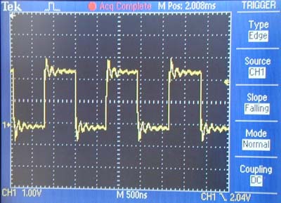
On an EFM32G890 chip running at 14MHz, outputting 0, 1, 0, 1, 0, 1 etc gave the following waveform:
Copyright © 2011 Crossware Products. All rights reserved.