Toggling an LED on a Kinetis K70 board

by Crossware 23. March 2016 12:32

Toggling a pin is one of the first things to do on a new microcontroller board.

Our board has an LED on port B pin 18 and the C code for toggling that pin is shown below.

The program is built to run in the SRAM of the K70 microcontroller avoiding the need to over-write anything in the on-chip flash memory.

main()
{
    // disable the watchdog timer
    g_pWDOG->UNLOCK = 0XC520;
    g_pWDOG->UNLOCK = 0XD928;
    g_pWDOG->STCTRLH &= ~WDOG_WDOGEN;
    // enable the PORTB module
    g_pSIM->SCGC5 |= SCGC5_PORTB;
    // set PTB18 to ALT1 (GPIO)
    g_pPORTB->PCR18 &= ~(PORT_MUX0 | PORT_MUX1 | PORT_MUX2);
    g_pPORTB->PCR18 |= 1 << 8;
    // set PTB18 as an output
    g_pGPIOB->PDDR = 1 << 18;
    while (1)
    {
        // toggle the PTB18
        g_pGPIOB->PTOR = 1 << 18;
        for (int i = 0; i < 100000; i++);
    }
}


Tags: , ,

Blog

Accessing on-chip memory from Javascript

by Crossware 27. February 2015 09:59

Today we updated the jState support within our Cortex-M3 and Cortex-M4 extensions to allow access to on-chip memory from Javascript.

The jState code creation wizard for the on-chip memory (accessible by right clicking on the Javascript file) will tell you what functions are available.

The image below shows code that it has created for us to set the on-chip memory read and write addresses to 0XE0000 and the increment on both read and write to 2.  (To increase the read or write address by 2 after each read or write.)


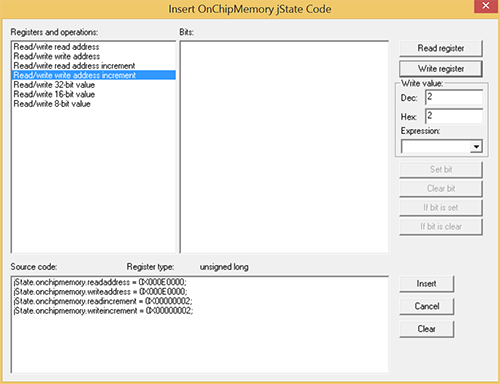
Clicking on Insert inserts this code into our Javascript file:

jState.onchipmemory.readaddress = 0X000E0000;
jState.onchipmemory.writeaddress = 0X000E0000;
jState.onchipmemory.readincrement = 2;
jState.onchipmemory.writeincrement = 2;


Our intension is to write a table of values into the on-chip flash memory sector at 0XE0000 - our simulating firmware is expecting this table to be in place at startup. So with a bit of manual editing we have the following Javascipt code:

console.clear();

PopulateTable()


function PopulateTable() {
    var TableData = [
        33, 38, 39, 44, 53, 55, 64, 69, 70, 75,
        156, 161, 162, 167, 176, 178, 187, 192, 193, 198,
        283, 288, 289, 294, 303, 305, 314, 319, 320, 325,
        411, 416, 417, 422, 431, 433, 442, 447, 448, 453,
        546, 551, 552, 557, 566, 568, 577, 582, 583, 589,
        661, 666, 667, 672, 681, 683, 692, 697, 698, 703]
    jState.onchipmemory.readaddress = 0X000E0000;
    jState.onchipmemory.writeaddress = 0X000E0000;
    jState.onchipmemory.readincrement = 2;
    jState.onchipmemory.writeincrement = 2;
    for (var i = 0; i < 60; i++) {
        jState.onchipmemory.value16 = TableData[i];
    }
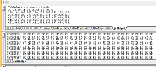
    console.log("TableData written to flash:");
    for (var i = 0; i < 60; i++) {
        if ((i % 10) == 0) {
            console.log("\n");
        }
        console.log(jState.onchipmemory.value16 + ",");
    }
}

When step into the simulator we can see that the data has been written into the correct memory locations:


By the way, to create the initial Javascript file select File->New and in the Files tab select Javascript Source File.  The Embedded Development Studio will populate the file name field for you so just click OK.

Tags: , , , , ,

Blog

Development Suite for ARM Enhancements

by Crossware 20. February 2015 09:32

The GUI parts of our Development Suite for ARM have been rebuilt using Microsoft's Visual Studio 2013.  That's over 80 DLLs as well as the Embedded Development Studio executable itself and so it was not an insignificant task.

For the embedded developer, this brings two major benefits:

1. The simulator can be graphically extended using Microsoft's latest Visual Studio 2013, including the free Community edition

2. The Cortex-M3 and Cortex-M4 simulations can also be extended using state-of-the art Javascript (see jState)

Unforunately it does mean leaving behind operating systems prior to Windows XP - the minimum requirement for these latest editions of the Development Suite for ARM is Windows XP SP3.

Tags: , , , , , , ,

Blog

More on Soft Switches of the ADSP-CM408F EZ-KIT Lite Board

by Crossware 27. August 2014 10:07

Continuing with my theme of yesterday where I wrote to the U40 MSP23017 soft switch chip to enable SW4 and SW5, I will show you how to read the register values from this U40 chip.

I've created two subroutines - WriteRegisterValue() and ReadRegisterValue() to make the main function clearer.

You will see below that I am writing to register 0X15 which is the output latch OLATB register whereas yesterday I wrote to register 0X13 GPIOB. But if you read back the value of register 0X13 after you have written to it, you do not see the value that you have written.  Instead you have to read OLATB to see this value.  The MSP23017 data sheet explains that a write to GPIOB is actually a write to OLATB and a read of GPIOB reads the port pins.  So to avoid confusion, I write directly to OLATB instead.

#include "xstdsys.h"

unsigned char regValues[0X16];

void WriteRegisterValue(unsigned char address, unsigned char value)
{
    g_pTWI0->MSTRCTL &= ~(TWI_MSTRCTL_DCNT0 | TWI_MSTRCTL_DCNT1 | TWI_MSTRCTL_DCNT2 | TWI_MSTRCTL_DCNT3 | TWI_MSTRCTL_DCNT4 | TWI_MSTRCTL_DCNT5 | TWI_MSTRCTL_DCNT6 | TWI_MSTRCTL_DCNT7);
    g_pTWI0->MSTRCTL |= 0X02 << 6;    // transmit 2 bytes
    g_pTWI0->MSTRCTL &= ~TWI_MSTRCTL_DIR;    // transmit
    g_pTWI0->TXDATA8 = address;
    g_pTWI0->MSTRCTL |= TWI_MSTRCTL_EN;
    while (g_pTWI0->FIFOSTAT & (TWI_FIFOSTAT_TXSTAT0 | TWI_FIFOSTAT_TXSTAT1));
    while ((g_pTWI0->ISTAT & TWI_ISTAT_TXSERV) == 0);
    g_pTWI0->ISTAT = TWI_ISTAT_TXSERV;
    g_pTWI0->TXDATA8 = value;
    while ((g_pTWI0->ISTAT & TWI_ISTAT_MCOMP) == 0);
    g_pTWI0->ISTAT = TWI_ISTAT_TXSERV | TWI_ISTAT_MCOMP;
}

unsigned char ReadRegisterValue(unsigned char address)
{
    // send register address
    g_pTWI0->MSTRCTL &= ~(TWI_MSTRCTL_DCNT0 | TWI_MSTRCTL_DCNT1 | TWI_MSTRCTL_DCNT2 | TWI_MSTRCTL_DCNT3 | TWI_MSTRCTL_DCNT4 | TWI_MSTRCTL_DCNT5 | TWI_MSTRCTL_DCNT6 | TWI_MSTRCTL_DCNT7);
    g_pTWI0->MSTRCTL |= 0X01 << 6;    // 1 byte
    g_pTWI0->MSTRCTL &= ~TWI_MSTRCTL_DIR;    // transmit
    g_pTWI0->TXDATA8 = address;
    g_pTWI0->MSTRCTL |= TWI_MSTRCTL_EN;
    while (g_pTWI0->FIFOSTAT & (TWI_FIFOSTAT_TXSTAT0 | TWI_FIFOSTAT_TXSTAT1));
    while ((g_pTWI0->ISTAT & TWI_ISTAT_TXSERV) == 0);
    while ((g_pTWI0->ISTAT & TWI_ISTAT_MCOMP) == 0);
    g_pTWI0->ISTAT = TWI_ISTAT_TXSERV | TWI_ISTAT_MCOMP;

    // read value
    g_pTWI0->MSTRCTL &= ~(TWI_MSTRCTL_DCNT0 | TWI_MSTRCTL_DCNT1 | TWI_MSTRCTL_DCNT2 | TWI_MSTRCTL_DCNT3 | TWI_MSTRCTL_DCNT4 | TWI_MSTRCTL_DCNT5 | TWI_MSTRCTL_DCNT6 | TWI_MSTRCTL_DCNT7);
    g_pTWI0->MSTRCTL |= 0X01 << 6;    // 1 byte
    g_pTWI0->MSTRCTL |= TWI_MSTRCTL_DIR;    // receive
    g_pTWI0->MSTRCTL |= TWI_MSTRCTL_EN;
    while ((g_pTWI0->FIFOSTAT & TWI_FIFOSTAT_RXSTAT0) == 0);
    while ((g_pTWI0->ISTAT & TWI_ISTAT_MCOMP) == 0);
    g_pTWI0->ISTAT = TWI_ISTAT_RXSERV | TWI_ISTAT_MCOMP;
    return (unsigned char)g_pTWI0->RXDATA8;
}

main()
{
    g_pTWI0->CLKDIV = 0XFFFF;
    g_pTWI0->MSTRADDR = 0X0020; // U40
    g_pTWI0->CTL = TWI_CTL_EN;

    WriteRegisterValue(0X15, 0X3E);    // write OLATB (output latch B)

    for (unsigned char address = 0; address <= 0X15; address++)
    {
        regValues[address] = ReadRegisterValue(address);
    }


    while (1)                   
    {
    }
}


Tags: , , ,

Blog

Switches and LEDs on the ADSP-CM408F EZ-KIT Lite Board from 'No Boot - idle' mode

by Crossware 26. August 2014 18:32

We like examples to be as simple as possible and this is as simple as we can make it for controlling both the switches and the LEDs on the ADSP-CM408F EZ-KIT Lite Board.

The switches SW4 and SW5 are disabled by default and so from a 'No Boot - idle' mode, the soft switches must be configured.  This means sending commands to the U40 chip using the TWI interface.

The TWI clock and data pins are not multiplexed and so there is no need to configure the GPIO in order to use them.

Possibly we could get away with fewer while loops in the code below and we could also run the TWI at a faster speed.  But it works as written and that should get you started.

Pressing SW4 turns on LED1 and turns off LED2.  Pressing SW5 turns on LED3 and turns off LED4.


#include "xstdsys.h"

#define DELAY 100000

#define LED1PIN 7
#define LED2PIN 6
#define LED3PIN 5
#define LED4PIN 9

#define SW4PIN 10
#define SW5PIN 8

main()
{
    g_pTWI0->CLKDIV = 0XFFFF;
    g_pTWI0->MSTRADDR = 0X0020;    // U40
    g_pTWI0->CTL = TWI_CTL_EN;

    // set register 13 (gpiob) U40 to 0X3E
    // register 1 (iodirb) defaults to 0XFF and so need not be configured
    g_pTWI0->MSTRCTL &= ~(TWI_MSTRCTL_DCNT0 | TWI_MSTRCTL_DCNT1 | TWI_MSTRCTL_DCNT2 | TWI_MSTRCTL_DCNT3 | TWI_MSTRCTL_DCNT4 | TWI_MSTRCTL_DCNT5 | TWI_MSTRCTL_DCNT6 | TWI_MSTRCTL_DCNT7);
    g_pTWI0->MSTRCTL |= 0X02 << 6;    // transmit 2 bytes
    g_pTWI0->TXDATA8 = 0X13;    // GPIOB
    g_pTWI0->MSTRCTL |= TWI_MSTRCTL_EN;
    while (g_pTWI0->FIFOSTAT & (TWI_FIFOSTAT_TXSTAT0 | TWI_FIFOSTAT_TXSTAT1));
    while ((g_pTWI0->ISTAT & TWI_ISTAT_TXSERV) == 0);
    g_pTWI0->ISTAT = TWI_ISTAT_TXSERV;
    g_pTWI0->TXDATA8 = 0X3E;     // leds and switches enabled
    while ((g_pTWI0->ISTAT & TWI_ISTAT_MCOMP) == 0);
    g_pTWI0->ISTAT = TWI_ISTAT_TXSERV | TWI_ISTAT_MCOMP;


    g_pPORTF->INEN_SET = 1 << SW4PIN;    // enable input
    g_pPORTE->INEN_SET = 1 << SW5PIN;    // enable input
    g_pPORTE->DIR_SET = 1 << LED1PIN;     // set as output
    g_pPORTE->DIR_SET = 1 << LED2PIN;     // set as output
    g_pPORTE->DIR_SET = 1 << LED3PIN;     // set as output
    g_pPORTE->DIR_SET = 1 << LED4PIN;     // set as output

    while (1)                   
    {
        if (g_pPORTF->DATA & (1 << SW4PIN))
        {
            g_pPORTE->DATA_SET = 1 << LED1PIN;
            g_pPORTE->DATA_CLR = 1 << LED2PIN;
        }
        else
        {
            g_pPORTE->DATA_CLR = 1 << LED1PIN;
            g_pPORTE->DATA_SET = 1 << LED2PIN;
        }
        if (g_pPORTE->DATA & (1 << SW5PIN))
        {
            g_pPORTE->DATA_SET = 1 << LED3PIN;
            g_pPORTE->DATA_CLR = 1 << LED4PIN;
        }   
        else
        {
            g_pPORTE->DATA_CLR = 1 << LED3PIN;
            g_pPORTE->DATA_SET = 1 << LED4PIN;
        }
    }
}

Tags: , ,

Blog

Toggling LEDs on ADSP-CM408F EZ-KIT Lite Board

by Crossware 26. August 2014 18:12

Here is the simplest example C program we can devise for toggling the LEDs on the ADSP-CM408F EX-KIT Lite Board.

All LEDs are on Port E.  By default the LEDs are enabled and so the soft switched do not need to be configured.  Only the GPIO directions need to be set to make them outputs.

#include "xstdsys.h"

#define DELAY 100000

#define LED1PIN 7
#define LED2PIN 6
#define LED3PIN 5
#define LED4PIN 9

main()
{
    // the following four lines could be combined into one if desired
    g_pPORTE->DIR_SET = 1 << LED1PIN;    // set as output
    g_pPORTE->DIR_SET = 1 << LED2PIN;    // set as output
    g_pPORTE->DIR_SET = 1 << LED3PIN;    // set as output
    g_pPORTE->DIR_SET = 1 << LED4PIN;    // set as output

    while (1)                   
    {
        for (volatile int i = 0; i < DELAY; i++);
        g_pPORTE->DATA_SET = 1 << LED1PIN;
        for (volatile int i = 0; i < DELAY; i++);
        g_pPORTE->DATA_CLR = 1 << LED1PIN;
        for (volatile int i = 0; i < DELAY; i++);
        g_pPORTE->DATA_SET = 1 << LED2PIN;
        for (volatile int i = 0; i < DELAY; i++);
        g_pPORTE->DATA_CLR = 1 << LED2PIN;
        for (volatile int i = 0; i < DELAY; i++);
        g_pPORTE->DATA_SET = 1 << LED3PIN;
        for (volatile int i = 0; i < DELAY; i++);
        g_pPORTE->DATA_CLR = 1 << LED3PIN;
        for (volatile int i = 0; i < DELAY; i++);
        g_pPORTE->DATA_SET = 1 << LED4PIN;
        for (volatile int i = 0; i < DELAY; i++);
        g_pPORTE->DATA_CLR = 1 << LED4PIN;
    }
}


Tags: , ,

Blog

Switches and LEDs on the ADSP-CM408F EZ-KIT Lite Board

by Crossware 15. August 2014 16:11

We are developing support for Analog Device's ADSP-CM40x microcontrollers.

We received our ADSP-CM408F EZ-KIT Lite board on Monday and set about investigating the operation of the JTAG/SWD debugger interface.  Pretty soon we could download and run programs in SRAM.  (Lots of omissions and errors in ADI's reference manual though so it took a lot longer to get there than it should have!)

As usual during such developments we incrementally work our way though the peripherals adding register definitions, simple context menu wizards, simulation and so on, testing that things work along the way.

There are lots of examples for this board provided by ADI but we couldn't find anything remotely simple.  So here is how to read the input switches SW4 and SW5 and illiminate the LEDs LED1 and LED 2:

// Initial CPP Source File
#include "xstdsys.h"

main()
{
    // use the Wizards (see Wizards menu) to configure the on-chip peripherals
    g_pPORTF->INEN_SET = 1 << 10;
    g_pPORTE->INEN_SET = 1 << 8;
    g_pPORTE->DIR_SET = 1 << 7;
    g_pPORTE->DIR_SET = 1 << 6;

    while (1)                   
    {
        if (g_pPORTE->DATA & (1 << 8))
            g_pPORTE->DATA_SET = 1 << 7;
        else
            g_pPORTE->DATA_CLR = 1 << 7;
        if (g_pPORTF->DATA & (1 << 10))
            g_pPORTE->DATA_SET = 1 << 6;
        else
            g_pPORTE->DATA_CLR = 1 << 6;
    }
}

Pressing SW4 illuminates LED2 and pressing SW5 illuminates LED1.  That's all there is to it if the board boots in the factory configuration (SPI master boot mode with POST installed).

However, the installed POST program has already configured the Soft Configuration switches.  To use the switches and LEDs from 'No Boot - idle' mode, the Soft Configuration switches must be configured.

Tags: , ,

Blog

About this blog

This is where you will find topical information that we think might be useful to you.

Month List